Precision Process Node Semiconductor Landing Page Template
Silicon is a scroll-reveal landing page template built for semiconductor and chip companies targeting hardware engineers, procurement leads, and startup CTOs. It presents 5nm, 3nm, and 2nm GAA process node specs in animated frosted-glass card layouts, pairs a rotating isometric chip die with a partner logo bar, and guides visitors toward a PDK trial signup or process brief download.
by Rocket studio
Quick summary
Silicon is a single-page, scroll-driven template designed for foundry and chip companies operating at the leading edge of semiconductor manufacturing. It opens with a rotating isometric die and a partner logo bar, then unfolds process node cards across 5nm, 3nm, and 2nm GAA nodes, each carrying full spec grids and animated comparison charts. The conversion goal is a PDK trial signup or a gated process brief download.
Who this template is for
This template speaks directly to the technical and commercial decision-makers who live inside the semiconductor manufacturing process. It is precise where they need precision and restrained where they need trust.
- Hardware engineers and IC designers evaluating process nodes for SoC or ASIC tape-out projects
- Procurement leads at consumer electronics firms comparing foundry partners and wafer volume commitments
- Startup CTOs designing a first custom ASIC on a tight budget who need spec depth before committing to a trial
What problem this template solves
Most foundry pages ask for a form before they prove anything. That approach loses the hardware engineer within the first scroll. The semiconductor manufacturing process is too complex and the stakes too high to ask for trust before demonstrating capability. This template inverts that order: specs, charts, and node comparisons appear first, and the call to action only becomes prominent once the visitor has absorbed enough technical depth to find it credible.
- Engineers leave pages that bury spec data behind gated content, costing the foundry a qualified lead
- Procurement leads cannot compare power consumption and transistor density across nodes without a structured layout that surfaces those numbers clearly
- Startup CTOs with limited budgets need to see manufacturing process maturity and lower cost pathways before clicking any trial button
What you get with this template
This is a fully structured, single-page layout with high-animation fidelity built for desktop-first semiconductor design audiences. Every section serves a specific job in the conversion flow, and the visual system is consistent from the hero to the footer.
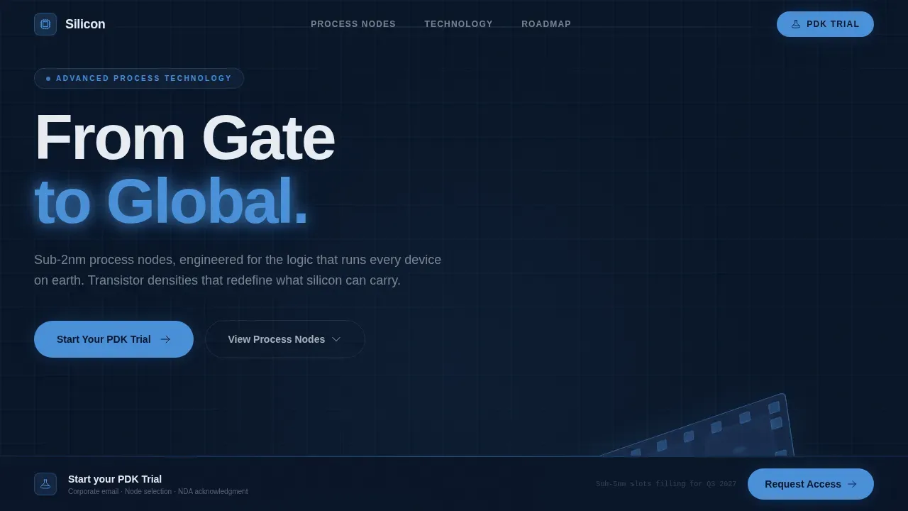
- A hero section with a rotating isometric chip die, a partner logo bar rendered in frosted glass, and a "From Gate to Global" headline in photon white
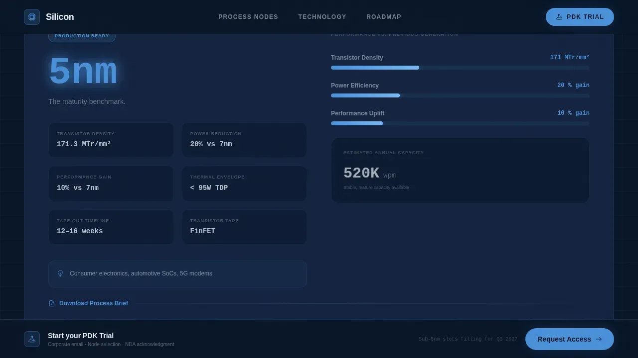
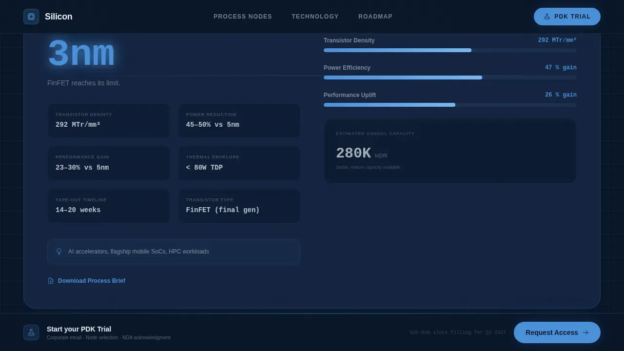
- Frosted-glass process node cards for 5nm, 3nm, and 2nm GAA, each containing structured spec grids covering transistor density, power efficiency, thermal envelope, and tape-out timeline
- Animated cathode-blue bar charts that fill on scroll entry, a roadmap section ending in a pulsing "Next" node, a sticky "Start Your PDK Trial" bar, a modal form, and a "Download Process Brief" secondary conversion path
Feature list
This template is built around a set of capabilities drawn directly from the brief. Each feature serves the manufacturing process audience and the freemium conversion goal.
Scroll-Reveal Process Node Matrix
As the visitor scrolls, each process node card slides up from a dark background like a wafer rising from an etch bath. The 5nm, 3nm, and 2nm GAA cards reveal in sequence, each carrying a full spec grid: transistor density, power consumption figures, thermal envelope, and tape-out timeline. This progressive reveal method creates a narrative of escalating capability that keeps engineers engaged through the full page.
Animated Comparison Engine
Each node card contains cathode-blue animated bar charts that fill on scroll entry, allowing cross-node analysis at a glance. This visual method of defining differences in power, speed, and area metrics communicates the semiconductor manufacturing process advantages more clearly than a static table ever could. Engineers evaluating process nodes can read the comparison without decoding dense documentation.
Rotating Isometric Chip Die
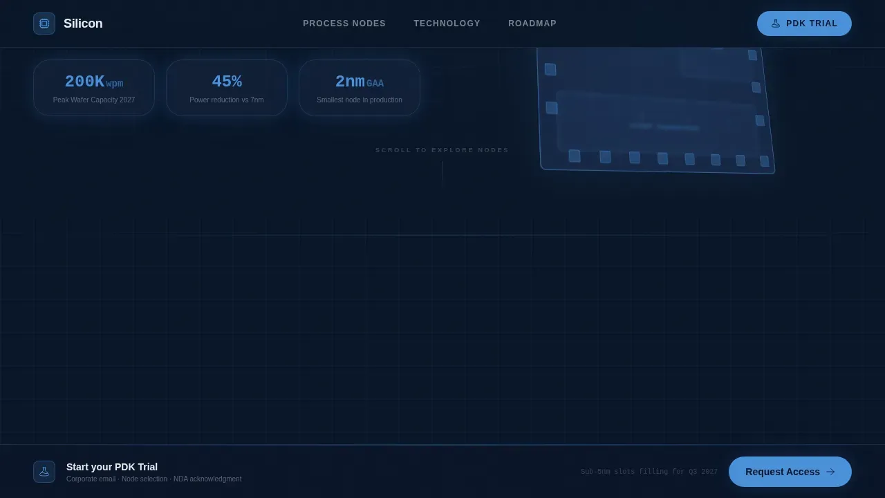
The hero section features a CSS three-dimensional chip die rotating slowly in isometric view. On hover, its metal layers separate to reveal the interconnect architecture beneath, giving visitors a visual image of what fabrication actually produces. This single interactive element establishes technical credibility before a single spec is read.
Partner Logo Bar with Cathode-Blue Backlight
A horizontal ribbon of partner and client logos sits above the headline, rendered in frosted glass white against the abyssal navy background. A faint cathode-blue backlight pulses gently behind each logo, creating the impression that these logos are powered by the chips themselves. This layout form communicates social proof without disrupting the cleanroom aesthetic.
Sticky PDK Trial Bar and Gated Process Brief
After the second node card reveals, a sticky bottom bar appears carrying the primary call to action: "Start Your PDK Trial." Clicking opens a modal form requesting a corporate email, target node selection, estimated annual wafer volume, and an NDA acknowledgment. A secondary "Download Process Brief" path appears beside each node card, gating a detailed process document behind just an email field to capture engineers not yet ready for a trial commitment.
Pulsing Roadmap Node
The roadmap section closes the main content area with a timeline ending in a node marked "Next." No specs are shown for this node; only a pulsing glow indicates something is coming. This design concept builds anticipation and gives returning visitors a reason to come back, keeping the foundry's pipeline visible without revealing premature details.
Page sections overview
| Section | Purpose |
|---|---|
| Hero Die Viewport | Rotating chip die, partner logo bar, and headline establish credibility instantly |
| 5nm Node Card | Spec grid for transistor density, power, thermal, and tape-out at 5nm |
| 3nm Node Card | Progressive reveal of denser, more efficient 3nm FinFET process specs |
| 2nm GAA Card | Leading-edge 2nm Gate-All-Around node with full comparison bar charts |
| Comparison Engine | Animated cathode-blue bar charts filling on scroll for cross-node analysis |
| Roadmap Timeline | Process node roadmap ending in a pulsing "Next" node with no specs yet |
| Sticky Trial Bar | Persistent "Start Your PDK Trial" call to action appearing after second card |
| Process Brief Gate | Email-gated "Download Process Brief" beside each node card |
| Modal Trial Form | Corporate email, node selection, wafer volume, and NDA toggle fields |
| Footer Flow | Dark horizontal footer following Vercel-style horizontal flow pattern |
Design & branding system
The visual identity is built on a Tech Glass aesthetic that feels like peering through a quartz viewport into a cleanroom at 2 a.m. Every color and typographic choice reinforces the precision and depth expected by semiconductor design professionals.
- Color palette: abyssal navy (#0A1628) as the primary background, deep sapphire (#162744) for card surfaces, cold cathode blue (#4A90D9) for interactive highlights and animated data lines, and photon white (#E8ECF1) for all primary typography and dividers
- Typography: Plus Jakarta Sans for headings and body text, JetBrains Mono for all spec data and numerical values, keeping engineering figures visually distinct from editorial copy
- Animation system: GSAP ScrollTrigger drives all scroll-reveal transitions, CSS three-dimensional rotation powers the chip die, animated bar charts fill on viewport entry, and cathode-blue pulsing glows appear on the logo bar and roadmap node
Mobile & speed optimization
Although the primary device target is desktop, where hardware engineers work on high-resolution workstations, the template is built with responsive layout behavior to accommodate mobile access.
- Desktop-first layout structure ensures that wide spec grids, comparison columns, and the three-dimensional chip die render with full fidelity on workstation screens
- Responsive breakpoints adapt node card grids, form modals, and the sticky trial bar for tablet and mobile viewports without breaking the visual hierarchy
How this template helps you convert
The conversion architecture follows a deliberate sequence: show depth first, then ask. By the time the call to action appears, the visitor has already evaluated multiple layers of technical evidence.
- The rotating chip die and partner logo bar establish foundry credibility before the first scroll, making the visitor confident that the technical content ahead is worth reading
- The progressive node card reveal delivers transistor density data, power efficiency figures, and thermal specs in a structured format that gives procurement leads and engineers the comparison framework they need to justify a trial request
- The sticky "Start Your PDK Trial" bar appears only after the second node card reveals, timing the ask to the moment when the visitor has already seen enough spec rigor to trust that the trial is worth their corporate email
Other information about this template
The Silicon template is specifically structured around the realities of the semiconductor manufacturing process. The eight-step manufacturing flow, from wafer processing through oxidation, photolithography, etching, film deposition, interconnection, testing, and packaging, forms the conceptual backbone of the content architecture. Understanding this flow helps teams populate the spec grids with accurate, process-relevant data.
- Wafer processing begins with the extraction of high-purity silicon from silica sand, formed into a single crystal ingot; the template's spec grids are designed to surface these substrate and material characteristics clearly
- The oxidation step forms a protective silicon dioxide layer on the wafer surface, building the oxide layer that prevents impurities; node cards can reference this in their electrical properties and reliability data fields
- Photolithography, the method of coating the wafer with photoresist and using lithography to create circuit patterns, and the subsequent etch process that removes excess material, are central to defining a node's design rules and minimum feature sizes
- Film deposition, including techniques such as chemical vapor deposition and atomic layer deposition, adds thin films of material to the wafer substrate to form the structures needed for transistors, capacitors, and other components
- Interconnection connects chip components using conductive material, typically aluminum or copper, allowing current flows between circuit elements; testing is then performed to find defects before packaging separates the wafer into individual units
- A Process Design Kit (PDK) bridges the design team and the foundry by packaging design rules, models, and verification decks; design flows rely on the PDK to create integrated circuits and to ensure every layout design adheres to manufacturing capabilities and electrical constraints
- PDKs are essential tools in semiconductor design, improving efficiency and minimizing manufacturing defects; they ensure a single chip design is manufacturable and meets the performance criteria set by the facility team before tape-out
- The template's visual system, including the scientist characters set illustrated in the brief's conceptual imagery, the facility team-facing micro processor performance displays, and the industrial manufacture equipment-themed card aesthetic, supports a range of semiconductor manufacturing process landing page contexts
- Smaller process nodes enable higher transistor density on a given wafer surface; leading-edge nodes such as 3nm and 2nm are used for artificial intelligence workloads and high-performance computing, while mature nodes remain critical for automotive and other devices requiring long-term supply reliability
- The semiconductor industry is increasingly relying on AI and machine learning to optimize design and manufacturing processes; this template's roadmap section is designed to signal forward momentum toward those next-generation process generations
- Chiplets and advanced packaging techniques are reshaping semiconductor design; the template's roadmap and node card structure can incorporate modular design narratives alongside traditional monolithic single chip presentations
- The scientist characters set used in conceptual illustrations across the semiconductor manufacturing process landing page ecosystem maps well to the facility team-oriented storytelling the Silicon template enables; teams can adapt image selections and scientist characters to reflect their own cleanroom personnel and industrial manufacture equipment
- The template supports the practice of displaying Power, Performance, and Area metrics prominently, which is a recognized standard for semiconductor manufacturing process landing pages targeting hardware engineering audiences
Theme
Tech Glass
Creative direction
Feature Matrix
Color system
Midnight Blue
Style
Scroll Reveal (Progressive)
Direction
Freemium/Trial
Page Sections
Scroll-reveal Process Node Matrix
Animated Cross-node Comparison Charts
Rotating Isometric Chip Die Hero
Sticky PDK Trial Bar and Modal Form
Email-gated Process Brief Download
Pulsing Roadmap Node with Anticipation Design
Related questions
What process node specifications does this template support?
How does the PDK trial form work?
Can a startup CTO use this template on a limited budget?
Is the template editable without deep coding knowledge?
Why does the sticky call-to-action bar appear only after the second node card?